Plenary Speakers
Plenary Speakers
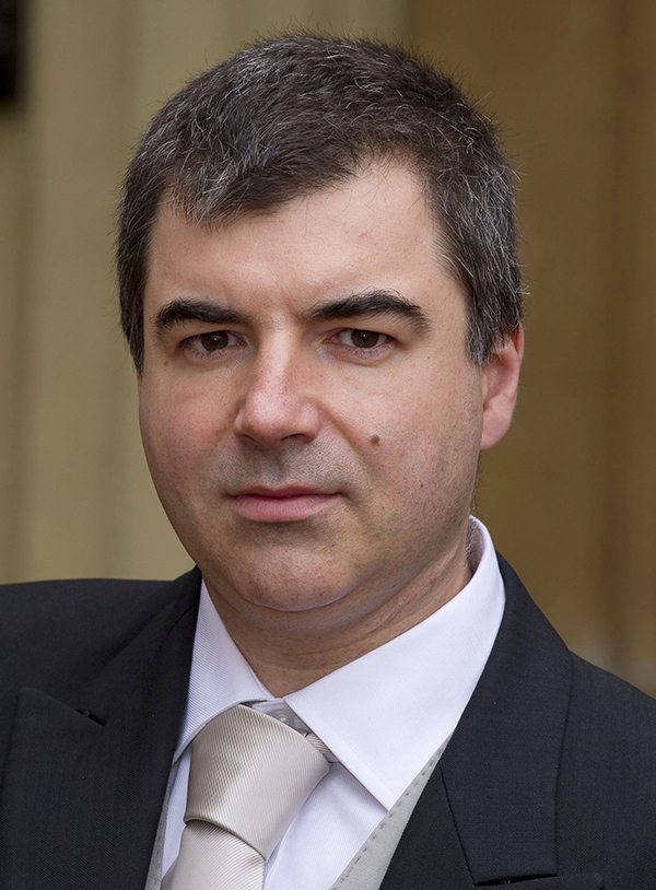
Konstantin Novoselov
National University of Singapore
Time: 6/18(Wed) 11:20-12:00
Place: Halla Hall

Deep Jariwala
University of Pennsylvania
III-Nitride Ferroelectric Materials: From Low-Power Memory to Extreme Environment Computing
Time: 6/16(Mon) 11:20-12:00
Place: Halla Hall
III-Nitride Ferroelectric Materials: From Low-Power Memory to Extreme Environment Computing
Since the demise of Dennard scaling, modern computer has largely relied on architectural innovations such as multi-core processors and GPUs vs CPUs to address the evolving needs of computing paradigm. This above problem has been exacerbated since computing has largely evolved from arithmetic centric to data centric in the age of billions of internet-connected devices and artificial intelligence. Thus, dense and reliable data storage combined with fast and high band-width access in novel memory devices has become the frontier for research in modern computing hardware. In this regard there have been several advancements across a variety of technologies in the past three decades. Ferroelectric materials and devices are among the forefront of these technologies due to their low-power and fast switching abilities but suffer from integration challenges. Simultaneously, developing data-heavy computing architectures in extreme environments is a growing need and a frontier challenge since silicon carbide (SiC) which is the leading logic technology for elevated temperature environments is limited by computing power and lack of memory devices that can operate at elevated temperatures.
Therefore, in this talk, I will try to make the case of how novel III-nitride materials might present interesting avenues to overcome some of the above limitations being faced by both Silicon and Silicon Carbide (SiC) hardware. I will start by presenting our ongoing and recent work on integration of 2D chalcogenide semiconductors emerging wurtzite structure ferroelectric nitride materials1 namely aluminium scandium nitride (AlScN). First, I will present on Ferroelectric Field Effect Transistors (FE-FETs) made from 2D materials when integrated with AlScN and make the case for 2D semiconductors in this application.2-4 I will then show our most recent results on scaling 2D/AlScN FE-FETs, achieving ultra-high carrier and current densities5 in ferroelectrically gated MoS2 and also demonstrate negative-capacitance FETs6 by engineering the AlScN/dielectric/2D interface.
Then, I will switch gears to introduce the ferroelectric diode (FeD) memory device7 and demonstrate multi-bit operation8 as well as compute in memory (CIM)9 using FeD devices made from AlScN. Finally, I will demonstrate why AlScN FeDs are uniquely suited as a high temperature non-volatile memory demonstrating stable operation upto 600 C10 and how AlScN can be integrated onto SiC11 for stable data retention in ferroelectric capacitors upto 800 C.12 I will end by providing a broad outlook on both AI computing hardware as well as high-temperature computing.13
References:
(1) Kim, K.-H.;et al. Jariwala, D. Nature Nanotechnology 2023, 18 (5), 422-441..
(2) Liu, X.; et al. Jariwala, D. Nano Letters 2021, 21 (9), 3753-3761.
(3) Kim, K.-H.; et al. Jariwala, D. Nature Nanotechnology 2023, 18, 1044–1050.
(4) Kim, K.-H.; et al. Jariwala, D. ACS Nano 2024, 18 (5), 4180-4188.
(5) Song, S.; et al. Jariwala, D. arXiv preprint arXiv:2406.02008 2024.
(6) Song, S.; et al. Jariwala, D. Applied Physics Letters 2023, 123 (18).
(7) Liu, X.; et al. Jariwala, D. Applied Physics Letters 2021, 118 (20), 202901.
(8) Kim, K.-H.;et al. Jariwala, D. ACS Nano 2024, 18 (24), 15925-15934.
(9) Liu, X.; et al. Jariwala, D. Nano Letters 2022, 22 (18), 7690–7698.
(10) Pradhan, D. K.; et al. Jariwala, D. Nature Electronics 2024, 7 (5), 348-355.
(11) He, Y.; et al. Jariwala, D. Applied Physics Letters 2023, 123 (12).
(12) He, Y.; et al. Jariwala, D. arXiv preprint arXiv:2411.16652 2024.
(13) Pradhan, D. K.; et al. Jariwala, D. Nature Reviews Materials 2024, 9 (11), 790-807.
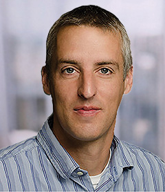
Graeme Henkelman
University of Texas at Austin
Computational methods for modeling reaction dynamics
Time: 6/17(Tue) 16:40-17:20
Place: Halla Hall
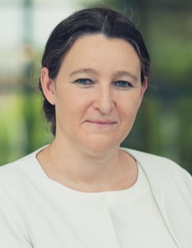
Inge Asselberghs
Interuniversity Microelectronics Centre
Towards manufacturing 2D-materials in an industry relevant environment
Time: 6/18(Wed) 17:20-18:00
Place: Halla Hall
Towards manufacturing 2D-materials in an industry relevant environment
Endless options for using 2D-materials in a multifold of applications, are the result of years of dedicated explorative research. The road to turn the academic achievements into industry uptake is long and requires innovation. Starting to use these new materials and processes in industry relevant environments provides good insights in the new materials and the process requirements. Here, we focus on wafer scale integration, mapping out possible integration routes and challenges addressed. While this is only the start, it can pave the way for uptake of 2D-materials by industry.
The 2D-PL pilot project is addressing some of these challenges and aims to build the ecosystem to enable 2D-materials integration focusing on photonics, sensors and electronic applications.
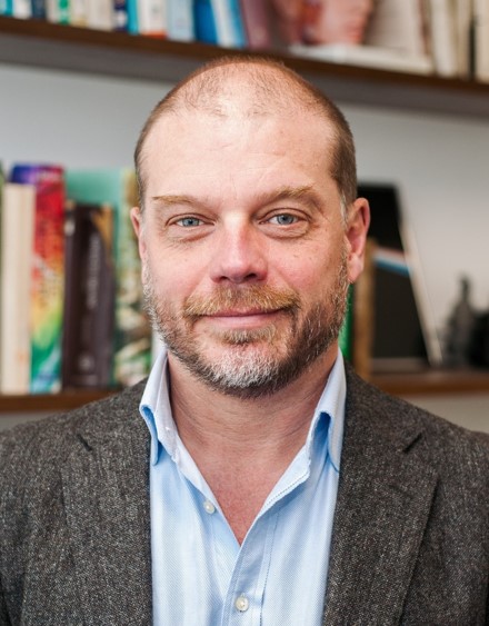
Nathan Gianneschi
Northwestern University
Ultrananoscale Proteomimetics: Protein-Scale Precision Materials for Cancer and Neurodegenerative Disease
Time: 6/17(Tue) 11:20-12:00
Place: Halla Hall
Ultrananoscale Proteomimetics: Protein-Scale Precision Materials for Cancer and Neurodegenerative Disease
We describe a pioneering approach to address areas of clinical unmet need. “Materials Biology” seeks to harness concepts in materials science and engineering to perturb, probe and drug cellular systems. These approaches do not include drug carriers or drug eluting entities; rather, they are materials capable of directly engaging with their targets (e.g., proteins, carbohydrates, nucleic acids) to probe and/or alter biological processes. Indeed, their function is often intrinsically linked to multivalency and macromolecular architecture mimetic of natural materials and complex protein systems. Hence, Materials Biology has as its analogue, “Chemical Biology,” a field that utilizes chemical tools to probe and perturb cellular/biological systems. Materials Biology emerges where small molecule probes and traditional antibody/biomolecule-based approaches have failed or continue to struggle. This has opened up opportunities for rethinking how we tackle key problems and questions in biology using materials at the same length scale as nature’s building blocks. For example, the problem of probing and disrupting complex protein-protein interactions (PPIs) occurring at the 0.1 to 10 nm length scale, between intrinsically disordered proteins and/or within protein aggregates and phase separated states that are more material than molecular in nature and behavior. Such complex, disordered proteins and indeed biological barriers including the skin and the BBB combine to severely limit the utility of traditional, large nanoparticles, small molecules and current biologics. We describe the development of new therapeutic material platform technologY with translational potential in oncology and incurable neurodegenerative disease.
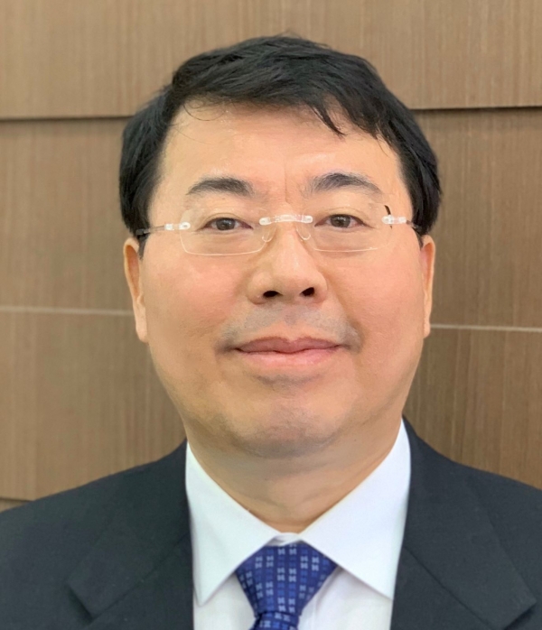
Wonyong Choi
Institute of Environmental & Climate Technology, Korea Institute of Energy Technology (KENTECH)
Designing and Modifying Photo(electro)catalytic Materials for Sustainable Environment
Time: 6/16(Mon) 16:40-17:20
Place: Halla Hall
Designing and Modifying Photo(electro)catalytic Materials for Sustainable Environment
Wonyong Choi*1
1Korea Institute of Energy Technology (KENTECH)
The global environment is challenged by excessive consumption of fossil fuels and resources, which perturbs the nature’s sustainable cycles of various chemical elements such as C, N, O, and H. As solar energy is the major driving force of the global cycles of these key elements, photo(electro)catalysis is an ideal engineering method to mimic and restore the nature’s element cycles. The photochemical conversion of H2O, CO2, N2, and O2 has been intensively investigated employing various methods among which photo(electro)catalysis using semiconductor materials has been established as the most popular method. This talk will introduce several examples of photocatalytic and photoelectrochemical (PEC) conversions of C, N, and O compounds and discuss their environmental implications. The photocatalytic and photoelectrocatalytic processes have been applied to denitrification, de-NOx, and nitrogen fixation reactions but the successful performance is limited. The direct conversion of nitrogenous pollutants to dinitrogen and dinitrogen to ammonia without using chemical reductants is an ideal solution but difficult to be realized. Here we introduce various engineered photo(electro)catalytic systems that selectively interconvert among NO3−, NO2−, NO, NH4+, and N2. As for O conversion, some examples of photocatalytic and photoelectrochemical systems for sustainable production of H2O2 through O2 reduction will be introduced. A PEC system enabled continuous H2O2 production over 100 h even under a bias‐free condition. As for CO2 conversion, a unique example that controls the selectivity of the multi-electron transfer mechanisms of CO2 transformation using heteronuclear dual-atom-site catalyst to generate an uncommon product (HCHO) will be discussed.
Keywords : Photocatalyst, Solar conversion, Photoelectrode, Water and air purification
Corresponding Author : Wonyong Choi (wchoi@kentech.ac.kr)


